Laser wafer dicing is a non-contact process for cutting wafers into individual dies. The benefits of this process include cost-effectiveness and non-contact processing. Challenges and opportunities remain, however. Here are some important factors to consider before using this process. First, it is crucial to have the correct starting point.
Non-contact processing
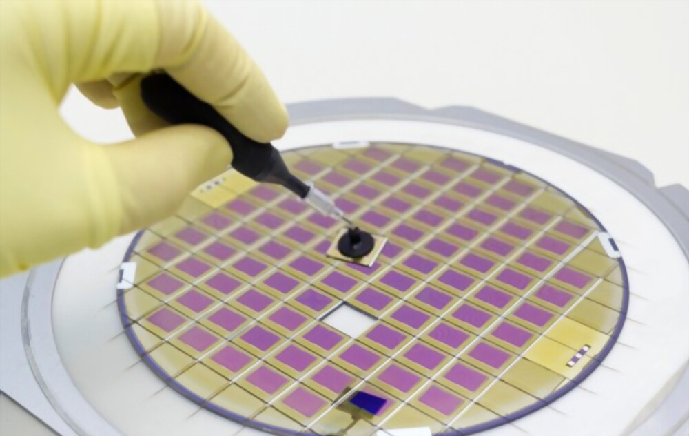
Non-contact laser wafer dicing is a process for separating a wafer into individual dies without touching the surface of the wafer. The process uses a semi-transparent wavelength of light to cut the wafer from the inside out. The wafer is first mounted on an adhesive to prevent movement. Then the laser is directed into a target area in the middle of the wafer. The laser breaks the wafer into individual dies by making a small crack in the wafer.
The process has advantages over traditional dicing techniques. For example, non-contact laser wafer dicing can be done on thin wafers that are less than 100um in thickness. This process also offers the benefits of compromised quality and high-speed cutting. Furthermore, non-contact laser dicing is easy to set up with a simple recipe, which can help improve production yield.
The process is carried out using a pulsed Nd-YAG laser, whose wavelength (1064 nm) matches the band gap of silicon. This wavelength can be adjusted optically for maximum absorption. Multiple laser scans are then performed on the wafer, in order to create defect regions with a 10 um width.
A non-contact laser wafer dicing system is highly efficient and can significantly reduce production costs. It can handle high-density wafers and can also control the heat generated by the laser. Its high repetition rate allows the laser to deliver high-power pulses while minimizing unwanted effects. In addition, high-repetition-rate lasers produce short laser pulses, which are ideal for efficient ablation.
Non-contact laser wafer dicing is becoming a popular method for wafer dicing. Its high-throughput, high-feed rate, and narrow kerf dicing process eliminate the need for dressing and tool wear. With non-contact laser wafer dicing, manufacturing costs can be reduced while improving the edge quality.
Non-contact laser wafer dicing is a method where a laser beam delivers high-intensity heat into a wafer’s surface. In addition to high-intensity heat, lasers can be focused on a particular region of the wafer, which causes localized voids. The weakened regions in the wafer act as perforations and break apart when the wafer is expanded.
Cost-effectiveness
Laser wafer dicing is a process used to separate layers of semiconductor material. Unlike the traditional wafer dicing process, it is non-contact and involves a low number of particles. In addition, laser-ablation dicing begins at the top surface and works its way down, removing layers layer by layer. The laser pulses are short, so heat is not transferred to adjacent atoms. However, the silicon that is ejected during the dicing process can heat the device.
In addition to this, laser dicing offers other advantages. The first is accuracy. The second advantage is cost-effectiveness. While laser dicing lacks the precision that is needed for high-volume dicing, the machine can process large volumes of material. Moreover, it is capable of delivering high throughput and high yield.
Another advantage of laser wafer dicing is its low energy consumption. The CO2 laser source delivers average powers of 500 W and can create 100-mm features on silicon. The downside is high thermal damage, so postprocessing is often necessary. Still, this cost-effective method is suitable for resizing wafers.
Laser dicing is also more expensive than the blade saw method. However, it can produce high-quality dies. This feature can improve feed rate and reduce street width. High repetition rate lasers also offer high peak power. This enables an efficient ablation process. However, they are more expensive and can result in lower overall system throughput.
Another advantage of laser dicing is its speed. Its higher speed can result in higher yields and is highly cost-effective. Laser dicing also requires less coating and DI water than other dicing technologies. Furthermore, it is environmentally friendly. Therefore, it is a cost-effective solution to thin wafer dicing.
There are two main approaches to laser wafer dicing. The first is based on the use of multiple lasers at the same time. The second involves a process called stealth dicing. This method forms a series of microcracks in the wafer, but no visible surface cracks are produced.
The cost-effectiveness of laser wafer dication is dependent on the application. Laser dicing offers a number of benefits for the semiconductor industry. First, it offers low initial investment and is widely used in the industry. Second, it enables you to achieve excellent yields, but it is not perfect. A bad reaction to the masking process can reduce the yield.
Challenges
The main challenges of laser wafer dicing are the mechanical stability of cut chips and the fast cutting speed of a wafer saw. This study analyzed the effects of laser process parameters on cutting quality and the number of dies produced. This method is suitable for processing thin 50-um silicon wafers.
The challenges of dicing include wafers with thin silicon and brittle GaAs substrates. Most traditional dicing methods use diamond blade saws and scribe tools to cut wafers. Laser wafer dicing has become a viable option with the advent of laser technology, especially for GaAs substrates.
The asynchronous dual laser beam method has been proposed as a solution to these problems. It involves two separate laser beams, one pulsed and the other continuous. The pulsed laser creates microcracks inside the wafer while the continuous laser generates thermal stress around the cracks. The continuous laser then separates the wafer. An FE model is used to study the thermal stress field and behavior of the dual laser beam dicing process.
Another challenge in laser wafer dicing is silicon wafer thickness. Since blade-based dicing is not ideal for thin silicon wafers, laser ablation is an alternative solution. The laser creates microcracks, which are difficult to clean up and result in weaker chips.
The study also looks at the influence of fluence, scan speed, and a number of scans on front and backside strength. The results of the fs-laser diced chips are better than those of the ns-laser diced ones. It is not clear whether fs-laser dicing is more reliable than ns-laser dicing, however.
Laser wafer dicing is a viable option for many applications and is able to overcome several common challenges that plague conventional wafer dicing processes. The main advantages are that it can be used on non-straight wafers. The process also eliminates the need to clean up debris and improves chip production yield. This makes it a great option for high-volume production.
Opportunities
Laser wafer dicing is a process that uses a laser to cut a wafer. This process is advantageous for the semiconductor industry because it reduces kerf loss and improves feed speed. This process is also advantageous for compound semiconductor wafers, as they tend to have more processing lines.
Laser wafer dicing uses a pulsed Nd-YAG laser. This laser has a wavelength that matches the silicon band gap. This wavelength can be tuned for maximum absorption. The laser beam is focused at different depths in a wafer, and multiple laser scans are performed to inscribe defect regions as small as 10 um in width.
The Global Laser Wafer Dicing Systems Market is segmented into two major regions: North America and Europe. In the North American region, the market is estimated to reach USD million by 2021. However, in Europe, the market is expected to reach USD million by 2028. This growth is projected to be due to the rising adoption of laser systems in manufacturing processes.
Laser full-cut dicing is another method of cutting a wafer. With this method, the laser beam can cut through the wafer from the inside out. Its benefits include increased UPH and processing speed. This technology is applicable to a wide range of materials, including GaP and backside metal film-attached Silicon wafers. This technology has the ability to support 300-mm-diameter wafers.
Plasma-based dicing is another technology that has significant advantages over traditional dicing techniques. This technology offers low-temperature, low-stress, and non-contact processes. But this non-contact method requires masking to remove non-etchable materials. This technique requires the use of a femtosecond-based laser scribe, plasma etching, and plasma dicing techniques.
Aside from reducing the time needed for cutting silicon wafers, it also improves the quality and yield. Unlike mechanical dicing, which can damage a wafer’s edge, laser-based dicing allows for a smooth and uniform cutting track. The dicing process requires high accuracy, high straightness, and high-velocity cutting.
Another technique, laser ablation, has the potential for chip manufacturing. The laser is highly concentrated and can remove material from a thin wafer, but it has its drawbacks. Laser ablation can be expensive and creates a kerf 14-inch wide. It also causes microcracks, which are difficult to clean up. Microcracks also make the chip less durable.
Thanks for visiting mwposting